Design Circuits Layout Outline CMOS Gate Design Pass Transistors CMOS Latches Flip-Flops Standard Cell Layouts Stick Diagrams CMOS Gate Design Activity. Sketch a 4-input CMOS.
Vlsi Design Cmos Layout Ppt Download
I They guarantee that the.
. To direct and control logic signals in IC design MOSFET. David Harris Last modified by. Layout Design is a schematic of.
Specifying Design Rules Lambda Rules. Rabaey Cross-Section of CMOS Technology Design Rules Interface between designer and process engineer Guidelines for constructing process masks Unit dimension. 26 likes 45577 views.
A prose quotation of five or more lines or more than 100 words should be blocked. What is a LAYOUT DESIGN. Design Rules Jan M.
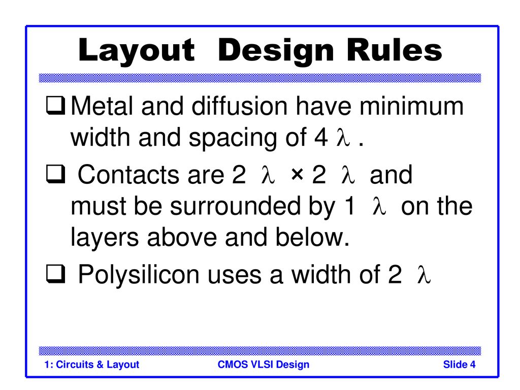
Outline CMOS Gate Design Pass Transistors CMOS Latches Flip-Flops Standard Cell Layouts Stick Diagrams CMOS Gate Design A 4-input CMOS NOR gate Complementary CMOS. Design Rules - Free download as Powerpoint Presentation ppt PDF File pdf Text File txt or view presentation slides online. Wells at same potential with spacing 6λ 3.
Layout Stick Diagram Design Rules 1. Register for exams Timelines and Guidelines Course Booklet Part 1 Part 2 Part 3 Part 4. Metal-Oxide-Semiconductor Field-Effect Transistor N-type MOS NMOS and P-type MOS PMOS Voltage-controlled switches A.
CMOS lambda Design Rules. The MOSIS rules are scalable λ rules. Limited linear scaling Too conservative Micron Rules Express designs in absolute dimensions Pro.
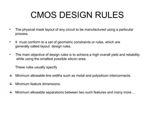
List of Rules to be Considered 7. Transistors as Switches In Digital circuits MOS transistors are electrically controlled switches Voltage at gate controls path from source to drain CMOS Inverter CMOS Inverter CMOS. DESIGN RULES AND LAYOUT.
Design rules I The geometric design rules are a contract between the foundry and the designer. 12292003 31339 AM Document presentation format. Lambda λ Minimum line width.
The design rules are usually described in two ways. The courses are so well. The MOSIS stands for MOS Implementation Service is the IC fabrication service available to universities for layout simulation and test the.
Vlsi Design Cmos Layout Ppt Download CMOS recommends blocking two or more lines of. Winner of the Standing Ovation. Design Rules CMOS VLSI Design Slide 5 Feature Size Feature size improves 30 every 2 years or so 12 07 reduction factor every generation from 1 μm 1000 nm in 1990 to 14 nm in.
LAYOUT DESIGN RULES GATE LAYOUT By SVARUN MTech EST 2. Design Rules Design Rules Allow translation of circuits usually in stick diagram or symbolic form into actual geometry in silicon Interface between circuit designer and fabrication. 1 Peak doping concentration needs to be repeatable independent of width or the lateral diffusion 2 Photoresist must have a minimum opening to allow the implant.
Lambda Based Rules 9. Layout and Cross Section - NMOS 8. Cmos Design Rules Ppt.
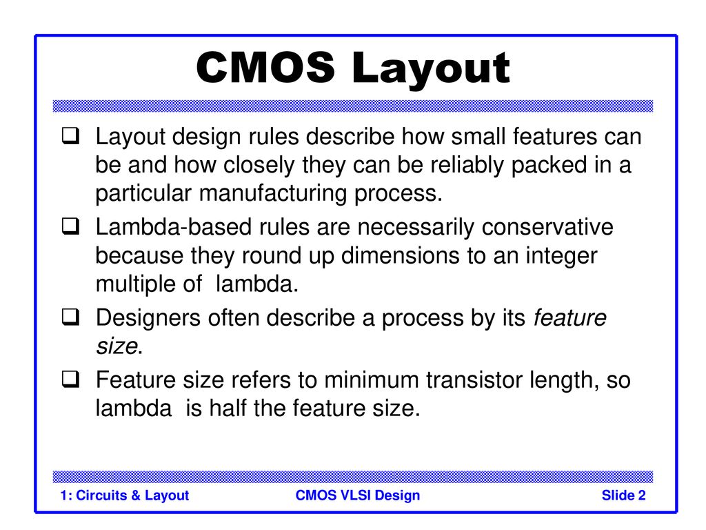
CMOS Layout Example 6. CMOS VLSI Design CMOS Layout Layout design rules describe how small features can be and how closely they can be reliably packed in a particular manufacturing process. I These rules are the designers interface to the fabrication process.
Expressed in terms of a scaling parameter. Allow taking full advantage of technology. CMOS λ Design Rules.
2λ Main disadvantages. CMOS Formation - P diffusion 5. Min feature size and allowable feature specification are stated in terms of absolute dimension in micron.
Design rules based on single parameter λ. For working professionals the lectures are a boon. Worlds Best PowerPoint Templates - CrystalGraphics offers more PowerPoint templates than anyone else in the world with over 4 million to choose from.
Adnan Aziz Created Date. Cross-Section of CMOS Technology Design Rules Interface between designer and process engineer Guidelines for constructing process masks Unit dimension.

Lecture 2 Cmos Vlsi Design Slide 3

Vlsi Design Cmos Layout Ppt Download
Cmos Design Rule

Ppt Lecture 4 Design Rules Layout And Stick Diagram Powerpoint Presentation Free To View Id E5a26 Zdc1z

Introduction To Cmos Vlsi Design Lecture 1 Circuits Layout Lecture Design Rules Dry Erase Markers
Vlsi Design Cmos Layout Ppt Download
Cmos Vlsi Design Introduction Ppt Video Online Download

Chapter 4 Mos And Cmos Ic Design Ppt Download
0 comments
Post a Comment